Since the power module has been developed, engineers have focused on how to make the modules smaller and lighter. In fact, we all understand that the power density of the product can be improved by increasing the switching frequency. But why has the volume of modules so far not changed much? What limits the switching frequency?
Under the guidance of market application, switching power products are increasingly demanding small, light, high efficiency, low radiation and low cost to meet all kinds of electronic terminal equipment. In order to meet the portable of electronic terminal equipment, the switching power must be small in volume and light weight. Therefore, the working frequency of switching power supply is improved. Rate has become a more and more concern for designers. However, what are the factors that restrict the upgrading of switching power supply? In fact, it mainly includes three aspects: switch tube, transformer and EMI and PCB design.
1. Switch frequency and switching frequency
As the core device of the switching power supply module, the switch speed and switching loss directly affect the limit of the switching frequency.
1. Switch speed
The loss of MOS tube is composed of switch loss and drive loss, as shown in Figure 1: open delay time TD (on), rise time TR, turn off delay time TD (off), and drop time TF.
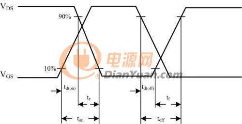
Figure 1 Schematic diagram of MOS tube switch
Take the MOS of FAIRCHILD company as an example, as shown in Figure 2: FDD8880 switch time characteristic table.
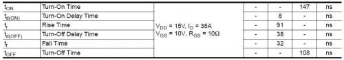
Figure 2 FDD8880 switch time characteristic table
For this MOS tube, its limit switching frequency is: fs=1/ (TD (on) +tr+td (off) +tf) Hz=1/ (8ns+91ns+38ns+32ns) =5.9MHz, in actual design, because the control switch duty ratio realizes the voltage regulation, so the switch tube's conduction and cut-off can not be completed instantaneously, that is, the actual limit switch frequency of the switch is far less than that of 5.9MHz, so the switch is open. The switching speed of the tube itself limits the increase of switching frequency.
2, switching loss
The corresponding waveform diagram, such as Figure 3 (A), and the corresponding waveform diagram such as Figure 3 (B) at the switch cut-off, can be seen that the switch tube VDS voltage and the current ID flow over the switch tube have overlapping time (yellow shadow position in the diagram), thus causing loss P1, so that the total of the switching frequency FS working state is total. Loss of PS=P1 *fs, that is, when the switching frequency is increased, the greater the number of switches and cut-off times, the greater the loss, as shown in Figure 3 below.
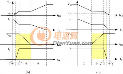
Figure 3 Diagram of switching tube loss
Two, transformer iron loss and switching frequency
The iron loss of transformer is mainly caused by eddy current loss of transformer, as shown in Figure 4.
When the coil is loaded with a high frequency current, a changing magnetic field is generated in the conductor and outside the conductor perpendicular to the current direction (1, 2 to 3 and 4 to 5 to 6) in the diagram. According to the law of electromagnetic induction, the changing magnetic field produces an induced electromotive force inside the conductor. The electromotive force produces eddy current (a, B, C, a, D, e to d) in the whole direction of the conductor (a, B, C, e, F, d) within the conductor, and the main current and eddy current are strengthened on the surface of the conductor, and the current tends to surface, then the effective intercepting area of the conductor is reduced, The conductors' AC resistance (eddy current loss coefficient) increases and the loss increases.
Figure 4 eddy current diagram of transformer
As shown in Figure 5, the transformer iron loss is proportional to the KF power of the switching frequency and is related to the limit of the magnetic temperature, so with the increase of the switching frequency, the high frequency effect is produced in the circulation of the high frequency current, which reduces the conversion efficiency of the transformer and causes the temperature increase of the voltage regulator, thus limiting the switching frequency. Improve.

Diagram 5 relation diagram of transformer iron loss and switch frequency
Three, EMI and PCB design and switching frequency
If the power device loss is solved, it is necessary to solve a series of engineering problems, because the inductor is not a familiar inductor at high frequency, and the capacitance is not the capacitance we have known. All the parasitic parameters will produce the corresponding parasitic effect, which seriously affects the performance of the power supply. The parasitic capacitance of the original side of the transformer, the leakage inductance of the transformer, the parasitic inductance and the parasitic capacitance between the PCB wiring will cause a series of voltage and current oscillations and EMI problems, and also a test of the voltage stress of the switch tube.
This article has been transferred to the Internet. If you have infringed upon your rights, please contact us and delete it in time.